Apple's Huge 3nm Chip Orders for iPhone 15 Pro and M3 Macs Helping to Maintain TSMC's Fab Utilization Rates

Apple supplier TSMC is making strides to improve its production capacity for chips based on its cutting-edge 3-nanometer process technology, according to industry sources, which is expected to debut in this year's iPhone 15 Pro and upcoming MacBook models.

tsmc semiconductor chip inspection 678x452
DigiTimes reports that TSMC's 5nm fabrication capacity began to loosen in November 2022 as a result of reduced orders from Apple, amongst other partners, with orders for iPhone chips alone having been slashed by 30%. However, the Taiwanese manufacturer has apparently been able to keep its utilization rate at 70% or higher thanks to Apple's thirst for 3nm:

TSMC continues to improve its capacity utilization for 3nm process technology, which is expected to approach 50% at the end of March, the sources said. The foundry will also grow the process output to 50,000-55,000 wafers monthly in March, with Apple being the main customer.

Apple's upcoming ‌iPhone 15 Pro‌ models are expected to feature the A17 Bionic processor, Apple's first ‌iPhone‌ chip based on TSMC's first-generation ‌3nm‌ process, also known as N3E.

The first-gen ‌3nm‌ process is said to deliver a 35% power efficiency improvement over TSMC's 5nm-based N4 fabrication process, which was used to make the A16 Bionic chip for the iPhone 14 Pro and Pro Max. The N3 technology will also offer significantly improved performance compared to current chips manufactured on 5nm.

Apple's next-generation 13-inch and 15-inch MacBook Air models are both expected to be equipped with an M3 chip, which is also likely to be manufactured on the ‌3nm‌ process for further performance and power efficiency improvements. Apple is also reportedly planning to release an updated version of the 13-inch MacBook Pro with an M3 chip. The M2 chip and its higher-end Pro and Max variants are built on TSMC's second-generation 5nm process.

Orders for new AI processors from Nvidia and AMD, as well as Apple's new ‌iPhone‌ chip, are expected to help TSMC avoid further fab utilization declines in the second quarter, DigiTimes' sources said.

Related Roundup: iPhone 15 Pro

Popular Stories

iPhone SE 4 Vertical Camera Feature

iPhone SE 4 Rumored to Use Same Rear Chassis as iPhone 16

Friday July 19, 2024 7:16 am PDT by
Apple will adopt the same rear chassis manufacturing process for the iPhone SE 4 that it is using for the upcoming standard iPhone 16, claims a new rumor coming out of China. According to the Weibo-based leaker "Fixed Focus Digital," the backplate manufacturing process for the iPhone SE 4 is "exactly the same" as the standard model in Apple's upcoming iPhone 16 lineup, which is expected to...
iPhone 16 Pro Sizes Feature

iPhone 16 Series Is Just Two Months Away: Everything We Know

Monday July 15, 2024 4:44 am PDT by
Apple typically releases its new iPhone series around mid-September, which means we are about two months out from the launch of the iPhone 16. Like the iPhone 15 series, this year's lineup is expected to stick with four models – iPhone 16, iPhone 16 Plus, iPhone 16 Pro, and iPhone 16 Pro Max – although there are plenty of design differences and new features to take into account. To bring ...
iphone 14 lineup

Cellebrite Unable to Unlock iPhones on iOS 17.4 or Later, Leak Reveals

Thursday July 18, 2024 4:18 am PDT by
Israel-based mobile forensics company Cellebrite is unable to unlock iPhones running iOS 17.4 or later, according to leaked documents verified by 404 Media. The documents provide a rare glimpse into the capabilities of the company's mobile forensics tools and highlight the ongoing security improvements in Apple's latest devices. The leaked "Cellebrite iOS Support Matrix" obtained by 404 Media...
tinypod apple watch

TinyPod Turns Your Apple Watch Into an iPod

Wednesday July 17, 2024 3:18 pm PDT by
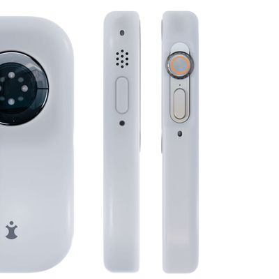
If you have an old Apple Watch and you're not sure what to do with it, a new product called TinyPod might be the answer. Priced at $79, the TinyPod is a silicone case with a built-in scroll wheel that houses the Apple Watch chassis. When an Apple Watch is placed inside the TinyPod, the click wheel on the case is able to be used to scroll through the Apple Watch interface. The feature works...
bsod

Crowdstrike Says Global IT Outage Impacting Windows PCs, But Mac and Linux Hosts Not Affected

Friday July 19, 2024 3:12 am PDT by
A widespread system failure is currently affecting numerous Windows devices globally, causing critical boot failures across various industries, including banks, rail networks, airlines, retailers, broadcasters, healthcare, and many more sectors. The issue, manifesting as a Blue Screen of Death (BSOD), is preventing computers from starting up properly and forcing them into continuous recovery...
New MacBook Pros Launching Tomorrow With These 4 New Features 2

M5 MacBook Models to Use New Compact Camera Module in 2025

Wednesday July 17, 2024 2:58 am PDT by
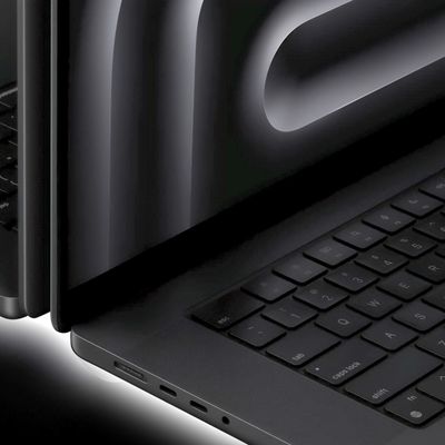
Apple in 2025 will take on a new compact camera module (CCM) supplier for future MacBook models powered by its next-generation M5 chip, according to Apple analyst Ming-Chi Kuo. Writing in his latest investor note on unny-opticals-2025-business-momentum-to-benefit-509819818c2a">Medium, Kuo said Apple will turn to Sunny Optical for the CCM in its M5 MacBooks. The Chinese optical lens company...

Top Rated Comments

iAFC Avatar
18 months ago

The industry is moving from nm to Ångströms. The node after 2 nm will be 18 å for example.
I'll finally find a use for this key on my Finnish keyboard.
Score: 20 Votes (Like | Disagree)
jdb8167 Avatar
18 months ago

What is the actual transistor size? I haven't been following that closely these past few years.
From Wikipedia:

The term "5 nm" has no relation to any actual physical feature (such as gate length, metal pitch or gate pitch) of the transistors being 5 nanometers ('https://en.m.wikipedia.org/wiki/Nanometer') in size. According to the projections contained in the 2021 update of the International Roadmap for Devices and Systems ('https://en.m.wikipedia.org/wiki/International_Roadmap_for_Devices_and_Systems') published by IEEE Standards Association Industry Connection, a "5 nm node is expected to have a contacted gate pitch of 51 nanometers and a tightest metal pitch of 30 nanometers".[3] ('https://en.m.wikipedia.org/wiki/5_nm_process#cite_note-3') However, in real world commercial practice, "5 nm" is used primarily as a marketing term by individual microchip manufacturers to refer to a new, improved generation of silicon semiconductor chips in terms of increased transistor density (i.e. a higher degree of miniaturization), increased speed and reduced power consumption compared to the previous 7 nm process ('https://en.m.wikipedia.org/wiki/7_nm_process').
https://en.m.wikipedia.org/wiki/5_nm_process


The term "3 nanometer" has no relation to any actual physical feature (such as gate length, metal pitch or gate pitch) of the transistors. According to the projections contained in the 2021 update of the International Roadmap for Devices and Systems ('https://en.m.wikipedia.org/wiki/International_Roadmap_for_Devices_and_Systems')published by IEEE Standards Association Industry Connection, a 3 nm node is expected to have a contacted gate pitch of 48 nanometers and a tightest metal pitch of 24 nanometers.[14] ('https://en.m.wikipedia.org/wiki/3_nm_process#cite_note-14')However, in real world commercial practice, "3 nm" is used primarily as a marketing term by individual microchip manufacturers to refer to a new, improved generation of silicon semiconductor chips in terms of increased transistor density (i.e. a higher degree of miniaturization), increased speed and reduced power consumption.[15] ('https://en.m.wikipedia.org/wiki/3_nm_process#cite_note-15')[16] ('https://en.m.wikipedia.org/wiki/3_nm_process#cite_note-16') Moreover, there is no industry-wide agreement among different manufacturers about what numbers would define a 3 nm node. Typically the chip manufacturer refers to its own previous process node (in this case the 5 nm process ('https://en.m.wikipedia.org/wiki/5_nm_process')node) for comparison. For example, TSMC has stated that its 3 nm FinFET chips will reduce power consumption by 25-30% at the same speed, increase speed by 10-15% at the same amount of power and increase transistor density by about 33% compared to its previous 5 nm FinFET chips.[17] ('https://en.m.wikipedia.org/wiki/3_nm_process#cite_note-17')[18] ('https://en.m.wikipedia.org/wiki/3_nm_process#cite_note-18') On the other hand, Samsung has stated that its 3 nm process will reduce power consumption by 45%, improve performance by 23%, and decrease surface area by 16% compared to its previous 5 nm process.
https://en.m.wikipedia.org/wiki/3_nm_process
Score: 16 Votes (Like | Disagree)
Aston441 Avatar
18 months ago
3 nanometer circuits... I still find this amazing. The first processor I ever experimented with was at 3500 nm. Not a typo.
Score: 13 Votes (Like | Disagree)
Aston441 Avatar
18 months ago

From Wikipedia:


https://en.m.wikipedia.org/wiki/5_nm_process
Holy crap! It's marketing BS ?

I thought something was off. Years ago I remember reading that below 5nm might be impossible due to quantum effects / hard physical reality.

Obviously marketing doesn't have those limitations.
Score: 11 Votes (Like | Disagree)
User 6502 Avatar
18 months ago

3 nanometer circuits... I still find this amazing. The first processor I ever experimented with was at 3500 nm. Not a typo.
it doesn’t seem real because it isn’t. The whole nm thing largely lost meaning and it has little to do with the actual transistor size. Sure there has been huge progress and they can squeeze so many more transistors in the same area than they used to, but 3nm is a misleading number. The truth is that we got to the limit of what’s physically possible: silicon atoms have a size and you can’t change that fact no matter how much research you do.
Score: 9 Votes (Like | Disagree)
jdb8167 Avatar
18 months ago

Does anyone else see what’s happening here? Eventually the nm will require floating point numbers, and these devices will be in more everyday devices running chatGPT 10.0 and replace us (although I think 100-200 year timeline on that last part, if not 5000).
The industry is moving from nm to Ångströms. The node after 2 nm will be 18 å for example.
Score: 7 Votes (Like | Disagree)